Boost Converter Circuit Principle and Parameter Design
Boost Converter Circuit Principle and Parameter Design
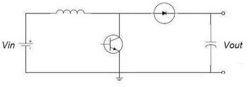
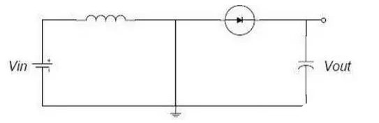
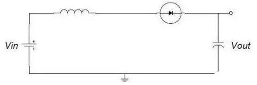
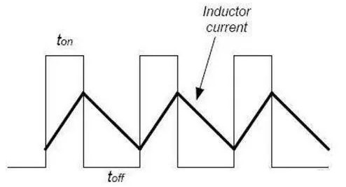
A Boost converter is a switching DC-DC boost circuit that enables the output voltage to be higher than the input voltage. It's a relatively common circuit design method in electronic circuit design. This article will introduce the basic principles and parameter design of the Boost converter. First, we need to know: Capacitors impede voltage changes, pass high frequencies, block low frequencies, pass AC, and block DC; Inductors impede current changes, pass low frequencies, block high frequencies, pass DC, and block AC; Figure 1 Schematic diagram of a Boost switching converter Assuming the switch (transistor or MOSFET) has been off for a long time, all components are in ideal conditions, and the capacitor voltage equals the input voltage. The circuit will be explained in two parts: charging and discharging. Charging Process During charging, the switch is closed (transistor conducts). The equivalent circuit is shown in Figure 2, with the switch (transistor) replaced by a wire. At this time, the input voltage flows through the inductor. The diode prevents the capacitor from discharging to ground. Since the input is direct current (DC), the current in the inductor increases linearly at a certain rate, which is related to the inductor's size. As the inductor current increases, some energy is stored in the inductor. Discharge Process Figure 3 shows the equivalent circuit when the switch is open (transistor is off). When the switch is open (transistor is off), due to the inductor's current-holding characteristic, the current flowing through the inductor does not immediately become zero, but slowly decreases from its fully charged value to zero. Since the original circuit is disconnected, the inductor can only discharge through the new circuit; that is, the inductor begins to charge the capacitor, increasing the voltage across the capacitor. At this point, the voltage is higher than the input voltage. The boost is complete. In essence, the boost process is an energy transfer process through an inductor. During charging, the inductor absorbs energy; during discharging, the inductor releases energy. If the capacitance is large enough, a continuous current can be maintained at the output during the discharge process. If this switching process is repeated continuously, a voltage higher than the input voltage can be obtained across the capacitor. Boost Circuit Boost Process The following are some supplementary points. For AA voltage converters, the bottleneck limiting power and efficiency lies in the switching transistor, rectifier diode, and other losses (including inductors). Inductors with too small a magnet (too little energy storage) or too thin a wire diameter (large pulse current leads to high line loss) are undesirable. Most rectifier diodes are Schottky diodes, which are all similar and lack distinctive features. At a 3.3V output, rectification losses are approximately 10%. The switching transistor is crucial. Sufficient amplification to reach saturation and a low on-state voltage drop are key to success. With only one volt, excessive dissipation in the transistor will result in no output current. Therefore, the transistor voltage drop should not exceed 0.2-0.3V at maximum current. If a single transistor cannot achieve this, multiple transistors should be connected in parallel. How large is the maximum current? Let's simply say 1A, but it's actually more. Due to low efficiency, it can exceed 1.5A (this is an average value). During half-cycle power supply, it's 3A, and the actual current waveform ranges from 0 to 6A. Therefore, it's recommended to use two transistors, supposedly rated 5A but actually only 3A, connected in parallel to barely handle the problem. No readily available chips integrate transistors with such high current, so a makeshift circuit is sufficient to handle the more advanced circuitry. These supplementary details are not found in textbooks, but they can be compared and verified with textbook content. When the switching transistor is on, the power supply forms a loop through the inductor and the switching transistor, where the current is converted into magnetic energy and stored. When the switching transistor is off, the magnetic energy in the inductor is converted into electrical energy, with the left side negative and the right side positive. This voltage is superimposed on the positive terminal of the power supply, forming a loop through the diode and the load to complete the boost function. Therefore, improving conversion efficiency requires addressing three aspects: minimizing the impedance of the loop when the switching transistor is on, maximizing the conversion of electrical energy into magnetic energy; minimizing the impedance of the load loop, maximizing the conversion of magnetic energy into electrical energy while minimizing loop losses; and minimizing the consumption of the control circuit, as the consumption of the control circuit is, in a sense, wasteful and cannot be converted into energy for the load. Boost Circuit Parameter Design For Boost circuits, the inductor current continuous mode differs significantly from the inductor current discontinuous mode. In discontinuous mode, the output voltage is related to the input voltage, inductor, load resistance, duty cycle, and switching frequency. In continuous mode, the output voltage depends only on the input voltage and duty cycle. Output Filter Capacitor Selection In switching power supplies, the output capacitor stores energy and maintains a constant voltage. The capacitor selection for Boost circuits primarily controls the output ripple within the specified range. For Boost circuits, the capacitor's impedance and output current determine the magnitude of the output voltage ripple. The capacitor's impedance consists of three parts: equivalent series inductance (ESL), equivalent series resistance (ESR), and capacitance (C). In continuous inductor current mode, the capacitor's size depends on the output current, switching frequency, and desired output ripple. When the MOSFET is turned on, the output filter capacitor provides the entire load current. Inductor In switching power supplies, the inductor stores energy. The function of an inductor is to maintain a constant current, or in other words, to limit the variation of current within the inductor. In boost circuits, selecting an appropriate inductance value is typically used to limit the ripple current flowing through it. The inductor's ripple current is directly proportional to the input voltage and the MOSFET's turn-on time, and inversely proportional to the inductance value. The inductance value determines the operating point in continuous and discontinuous modes. Besides the inductance value, the maximum DC or peak current and the maximum operating frequency should also be considered when selecting an inductor. Exceeding the inductor's rated current or operating frequency beyond its maximum operating frequency will lead to inductor saturation and overheating. MOSFETs are the most commonly used power switches in low-power DC/DC converters. MOSFETs are relatively inexpensive and operate at relatively high frequencies. The selection of a MOSFET in a design primarily considers its conduction and switching losses. The MOSFET should have a sufficiently low on-resistance RDS(ON) and a relatively low gate charge Qg.