

Product Overview
The PDL-1000 is a specialized analytical platform designed to solve the measurement challenges of next-generation materials with extremely low signal-to-noise ratios.
| Quick Specifications | |
|---|---|
| Mobility Range | Able to handle < 0.1 cm²/Vs |
| Magnetic Field | ~2.5 T pk-pk (AC Field) |
| Field Uniformity | < 2% over 10x10 mm area |
| Operating Modes | AC and DC Hall Measurement |
| Form Factor | Compact Tabletop System |
| Software | Proprietary UI with Auto-Extraction |
Key Features
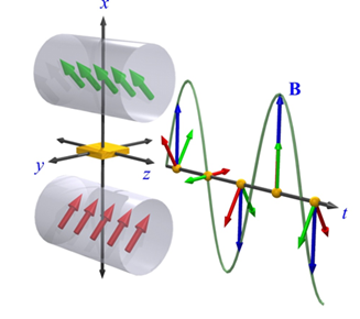
AC Field PDL Technology
Utilizes a rotating parallel dipole line to generate high-intensity oscillating magnetic fields, which is the core innovation for high-sensitivity detection.
- Enables high-resolution measurement of mobility < 0.1 cm²/Vs
- Eliminates thermal drift and offset voltages through AC modulation
- Produces a large, consistent peak-to-peak field of ~2.5 T
Proprietary Signal Processing
Features advanced software algorithms and hardware integration designed to extract valid signals from extremely noisy environments.
- Integrated Lock-in amplification for synchronous signal detection
- Sophisticated background subtraction for highly resistive films
- Real-time visualization of Hall coefficients and voltage curves
Automation & Integration
Designed for professional research environments where reproducibility and ease of use are paramount for data validation.
- Fully automated parameter extraction for Carrier Density and Mobility
- Software-controlled gate bias voltage option for FET characterization
- Built-in contact verification to ensure measurement integrity
Research-Grade Precision
A compact tabletop solution that delivers the performance of large superconducting magnets without the associated costs or space requirements.
- Exceptional field uniformity (< 2%) across the entire measurement area
- Low-maintenance design suitable for multi-user academic and industrial labs
- Versatile sample handling for semiconductors, thermoelectrics, and PVs
Technical Specifications
| Technical Parameter | Specification Detail |
|---|---|
| Minimum Mobility Limit | < 0.1 cm²/Vs (Industry-leading sensitivity) |
| Magnetic Field Strength (AC) | ~ 2.5 T pk-pk (Enables strong signal modulation) |
| Field Uniformity | < 2% (Maintained for sample sizes up to 10x10 mm) |
| Available Measurement Modes | AC Field Hall & DC Field Hall (Versatile characterization) |
| Gate Voltage Integration | Software-controlled Gate Bias (Optional upgrade) |
| Primary Extracted Parameters | Carrier Concentration, Mobility, Sheet Resistance |
| Operating Software Suite | Proprietary Semilab UI / Advanced Signal Processing |
| System Form Factor | Compact Tabletop Configuration (Space-saving design) |
| Signal Extraction Technique | High S/N Lock-in extraction & Background subtraction |
| Material Compatibility | PV absorbers, Thermoelectrics, Wide Bandgap Semiconductors |
Application
Photovoltaic Research
Characterizing low-mobility absorbers such as Perovskites, CIGS, and CZTS, as well as evaluating the uniformity and electronic quality of Transparent Conductive Oxides (TCOs).
Semiconductor Analysis
Investigating the electronic transport properties of wide-bandgap materials (GaN, SiC) and high-resistance oxide semiconductors used in advanced TFT and power electronics.
Thermoelectric Materials
Measuring carrier concentration and mobility in high-efficiency thermoelectric materials to optimize the power factor and overall figure of merit (ZT) for energy harvesting.
