

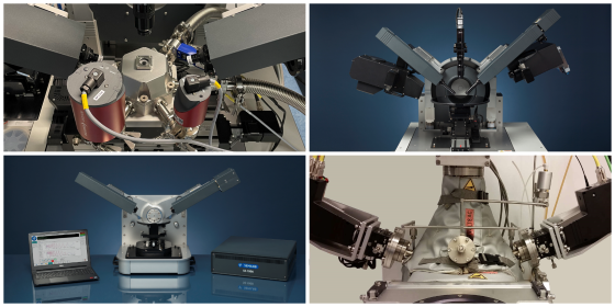
Product Overview
The SE-2000 is a modular spectroscopic ellipsometer platform that provides the widest spectral range in a single tool, covering wavelengths from 190 nm up to 25 µm.
Key Specifications
| System Parameters | |
|---|---|
| Spectral Range | 190 nm to 25 µm (UV to Mid-IR) |
| Electronics | Semilab Smart Interchangeable |
| Software | SAM/SEA Next-Gen Generation |
| Goniometer | High-Precision Automated |
| Mapping | Fully Automated Stage Options |
| Metrology | Expandable Multi-Sensor Integration |
Core System Features
Uniquely spans from Deep-UV through Visible to Mid-Infrared, allowing for characterization of materials across all optical regimes.
Features Semilab’s modular electronics platform with interchangeable components, facilitating rapid maintenance and hardware scalability.
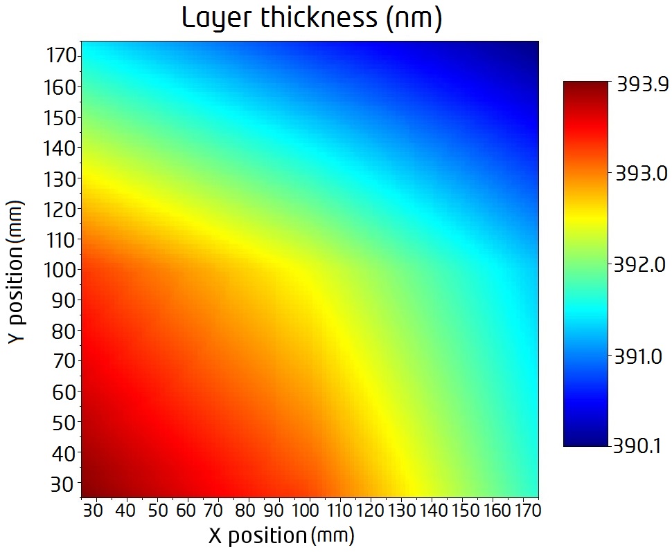
Equipped with fully automated goniometers and mapping stages to ensure high throughput and repeatability for industrial applications.
Designed to host additional metrology sensors such as 4-point probe or Eddy Current, creating a centralized characterization hub.
Supports Mueller Matrix (up to 16 elements), Generalized Ellipsometry, and scatterometry for complex 3D structures.
Utilizes pure optical interaction to measure samples without contact, preserving the integrity of sensitive substrates.
Technical Specifications
| Technical Parameter | Specification Detail |
|---|---|
| Standard Spectral Coverage | 190 nm – 2500 nm (Extensions up to 25 µm) |
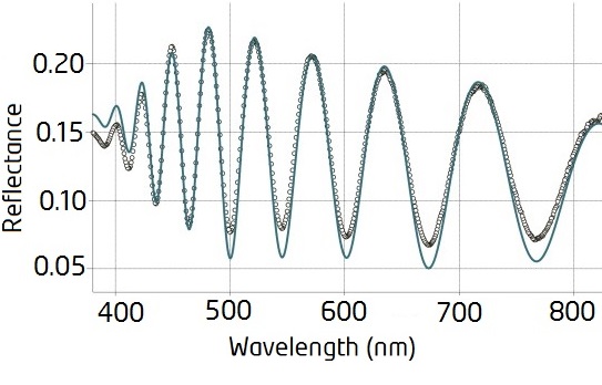
| Core Technology | Spectroscopic Ellipsometry with Rotating Compensator |
| Advanced Modes | Mueller Matrix (11 or 16 elements), Generalized Ellipsometry |
| Goniometer | Fully Automated Angle of Incidence adjustment |
| Stage Mapping | Automated X-Y mapping for large area uniformity checks |
| Electronics Platform | New generation Smart Electronics (Interchangeable) |
| Operating Suite | SAM/SEA software for measurement and sophisticated analysis |
| Sensor Capability | Expandable to 4pp, Eddy Current, and Reflectometry |
| Physical Parameters | Thickness, n and k constants, Porosity, Bandgap |
| Metrology Type | Scatterometry for 3D Periodic Structures |
Scientific & Industrial Applications
Semiconductor Manufacturing
Precise metrology for high-k dielectrics, photoresists, and complex transistor gate stacks in logic and memory nodes.
Display Technology
Characterization of multi-layer OLED stacks, TCO layers, and color filter materials for high-resolution panels.

Photovoltaics & Solar
Monitoring anti-reflective coatings and passivation layers to maximize efficiency in next-gen solar cells.
