DLS-1100 Deep Level Transient Spectrometer

DLS-1100 Deep Level Transient Spectrometer

Category: SEMILAB Available
For more information, visit our official website at atomic-solutions.net

Description

DLS-1100 Deep Level Transient Spectrometer

The DLS-1100 Deep Level Transient Spectrometer is a premier metrology platform designed for characterizing electrically active defects and lattice impurities in semiconductor materials. Integrating low-vibration cryostat technology with advanced signal processing, it enables automated measurement of trap concentration, activation energy, and capture cross-sections. Engineered for wafer manufacturers and research institutes, the DLS-1100 provides critical data to ensure optimal carrier performance and material purity.

Product Overview

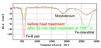
Deep Level Transient Spectroscopy (DLTS) is essential for identifying traps that limit device efficiency. The DLS-1100 supports comprehensive measurement modes including temperature scans, frequency scans, and depth profiling. With high-speed digitization of capacitance transients, it provides detailed numerical evaluations via a specialized Transient Recorder.
The system is built for versatility, accommodating both standard Capacitance DLTS and Current-based DLS (I-DLS) for conductive samples. Improved evaluation software automates experimental control, allowing precise characterization of impurity levels across a wide thermal range.

Core Features

  • High-Sensitivity Detection: Capable of identifying trace level contaminants down to 5 x 10⁷ atoms/cm3 for high-purity material validation.
  • Numerical Evaluation: Automated numerical analysis of digitized capacitance transients for accurate determination of trap properties.
  • Multi-Sensor Thermal Control: Features up to 10 sensors ensuring temperature measurement accuracy of less than 1 K across the testing range.
  • Dual Analysis Modes: Integrated support for both Capacitance DLTS and I-DLS, tailored for high-conductivity semiconductor samples.
  • Automated Logic: Fully automatic control of experimental parameters and calculation of trap concentration and activation energy.

Application

Wafer Manufacturing

Verification of semiconductor purity and monitoring of metallic contaminants during production to ensure high-yield device fabrication.

Photovoltaics (DLTS-PV)

Characterization of recombination centers in solar materials to optimize charge carrier lifetime and energy conversion efficiency.

MOS Structure Analysis

Evaluating interface state densities and deep level traps in Metal-Oxide-Semiconductors to improve gate oxide stability.

Technical Specifications

Technical Parameter Specification Detail
Impurity Detection Sensitivity 5 x 10⁷ atoms/cm3
Thermal Stability Advanced controller maintaining < 1 K error
Cryostat Option: Closed He 30 K to 325 K Range
Cryostat Option: Bath Nitrogen 77 K to 450 K Range
Cryostat Option: Auto Flow 80 K to 550 K or 80 K to 800 K Range
Measurement Core Lock-in Integrator for Capacitance Transients
Advanced Logic Digitization and Numerical Analysis via Transient Recorder
Trap Identification Activation Energy and Capture Cross Section Evaluation
Conductivity Adaptation Current DLS (I-DLS) for low-impedance samples
Software Architecture Win-based platform for automated measurement and report generation

Advantages

Elite Sensitivity Detects trace impurities down to 5x10⁷ atoms/cm3, allowing for proactive identification of defects that impact device reliability.
Process Automation Minimizes operator error through improved software that automatically manages temperature cycles and trap evaluation.
Vibration-Free Precision Advanced cryostat chambers ensure ultra-low vibration levels, maximizing signal-to-noise ratios for sensitive research measurements.
Direct Numerical Insights Full transient digitization provides statistically sound data on activation energy and trap concentration for high-level technical reporting.
Material Flexibility Versatile measurement modes support a wide range of semiconductor types, from wide-bandgap materials to PV solar cells.
Optimized Metrology Scalable architecture facilitates both laboratory-scale R&D and high-purity wafer quality control in industrial settings.

More detail about Atomic Solutions Sdn Bhd
Atomic Solutions Sdn Bhd
Atomic Solutions Sdn Bhd Lab Equipment Supplier Johor Bahru (JB), Scientific Instrument Supply Selangor, KL, Scanning Electron Microscope Supplies Malaysia, Penang ~ Atomic Solutions Sdn Bhd
Contact Us flagMalaysia