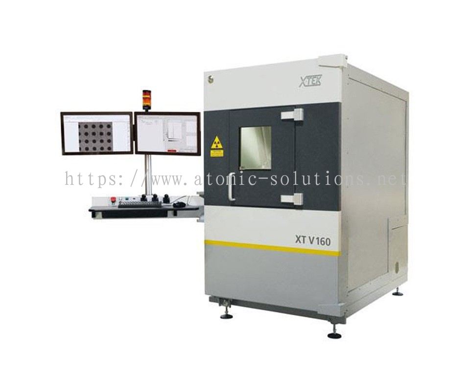

XT V Series X-ray and CT Systems
The XT V series enables insights into printed circuit board assemblies, components, or electrical devices in an intuitive, non-destructive inspection process. Designed to cope with ever-shrinking geometries and tighter quality standards, these systems accelerate throughput and improve product quality while reducing costs through high-resolution imaging and flexible 3D packaging analysis.
System Overview
Configuration Options
- Source Type Open-tube Nano-focus
- Detector FPD / 16-bit Imaging
- Axis Control 5-Axis Manipulator
- Compliance CE / Radiation Safety
Key Advantages
Real-time Imaging
The high-speed imaging chain allows for real-time visualization of internal structures, enabling immediate defect detection and process control.
Computed Tomography
Optional CT capability allows for 3D reconstruction, providing a deeper understanding of complex components and hidden solder joints.
Intuitive Operation
Easy-to-use software with automated inspection routines ensures high productivity for both experienced users and novices.
Multi-Axis Movement
Precision 5-axis manipulation enables views from any angle, essential for inspecting 3D packaging and multi-layered assemblies.
Technical Specifications
| Feature | XT V 160 | XT V 130C |
|---|---|---|
| X-ray Source | ||
| Max kV | 160 kV | 130 kV |
| Max. electron beam power | 20 W | 10 W |
| X-ray source | Open tube transmission target | |
| Focal spot size | 1 μm | 3 μm |
| Feature recognition | 500 nm | 2 μm |
| Geometric magnification | 2,046x | |
| System magnification | Up to 36,000x | |
| Imaging system | Varex 2520DX (2.85 Mpixel, 16-bit) Flatpanel Varex 1515DX (1.3 Mpixel, 16-bit) Flatpanel |
Varex 1313DX (1 Mpixel, 16-bit) Flatpanel |
| Manipulator & System | ||
| Manipulator | 5-axis (X, Y, Z, T, R) | 4-axis (X, Y, Z, T) |
| Rotate axis | Included | Optional |
| Tilt | 0 - 72 degrees | |
| Measuring volume | Largest square in single map 406 x 406 mm (16 x 16") Maximum physical sample size 711 x 722 mm (28 x 30") |
|
| Max. sample weight | 5 kg (11 lbs) | |
| Enclosure, Controls & Software | ||
| Monitor | Single 4k IPS (3,840 x 2,160 pixels) | |
| Cabinet dimensions (W x D x H) | 1,200 x 1,786 x 1,916 mm (48.0 x 71.3 x 75.4") | |
| Weight | 2,100 kg (4,629 lbs) | |
| Radiation safety | <1 μSv/hr at the cabinet surface | |
| Control | Inspect-X control and analysis software | |
| Automated inspection | Included | Optional |
| Computed Tomography / X.Tract | Optional | |
| Primary applications | Real-time and automated electronics and semiconductor inspection, failure analysis | Real-time electronics inspection |
Highlights
Versatile Applications
Surface Mount Devices
Analysis of BGA, QFN, QFP, and CSP components for diameter, circularity, and voiding.
Through-Hole Inspection
Verification of solder filling in PTH, detecting cracks, and checking for bridging between pins.
IC Bonding
High-resolution inspection of gold or copper wire bonding, flip chip, and C4 connections.
Failure Analysis
Non-destructive characterization of electrical devices and multi-layer PCB assemblies.
