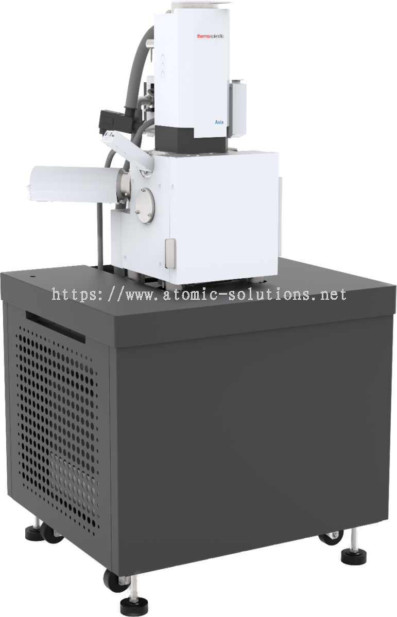

Thermo Scientific™ Axia™ ChemiSEM
Instant fusion of chemistry and imaging — live quantitative elemental mapping activates the moment the electron beam turns on. The first SEM-EDS platform where chemical data and imaging are inseparable, designed for both expert microscopists and first-time users.
Product Overview
The Thermo Scientific Axia ChemiSEM redefines scanning electron microscopy by fully integrating SEM imaging and energy dispersive X-ray spectroscopy (EDS) into a single cohesive platform. Built on ChemiSEM Technology — a tight hardware-software co-design — the system uses a single scan generator to simultaneously control SE/BSE imaging and X-ray acquisition, ensuring perfectly co-registered data from the very first scan. Elemental composition is displayed as color directly in the SEM image the moment the beam turns on, quantified at every pixel and accessible through a simple tooltip — eliminating complex, multi-step EDS workflows entirely.
Designed for industrial R&D, failure analysis laboratories, materials characterization centers, and academic research institutions, the Axia ChemiSEM reduces analysis time by up to 50% compared to conventional SEM-EDS workflows. SmartAlign technology manages all column alignments automatically, keeping the system permanently calibrated and ready to image. Built on a completely new mechanical platform, the system accommodates samples up to 10 kg with full-door chamber access, removing the need for destructive sample preparation. The result is a system equally capable in the hands of a first-time user as it is for an experienced electron microscopist — delivering complete chemical and morphological information faster than any conventional SEM-EDS combination.
Main Features & Capabilities
Live Quantitative Elemental Mapping
ChemiSEM Technology delivers per-pixel elemental composition the instant the beam activates. Colors in the image represent element distribution — quantified at every pixel and readable via tooltip — eliminating conventional post-processing EDS workflows entirely. Full quantitative elemental maps are generated in as little as 30 seconds.
Alignment-Free Operation (SmartAlign)
SmartAlign technology automatically manages all column parameters — gun tilt, gun shift, and beam alignment — every time accelerating voltage or imaging conditions change. The system is always calibrated and ready to image without operator intervention, eliminating a major source of workflow friction for new and experienced users.
Nav-Cam Camera & Navigation Montage
The integrated Nav-Cam color optical camera enables point-and-click navigation directly on a color image of the sample. Navigation Montage automatically stitches multiple SE/BSE frames — with simultaneous EDS acquisition — into a large-area overview for rapid screening and region-of-interest identification.
Flexible Sample Loading
Full-door chamber access and a 5-axis motorized stage accommodate samples up to 10 kg, 280 mm in diameter, and 138 mm in height — the largest sample capacity of any SEM in its class. Accepts up to 7 sample stubs simultaneously; beam ready in under 2 minutes after loading.
Multi-Detector Simultaneous Acquisition
Detects up to 4 signals simultaneously from any combination of ETD (SE), dual-segment retractable BSE, TrueSight X EDS, low-vacuum SE, RGB cathodoluminescence, and optional EBSD — all controlled and visualized from a single unified user interface without mode switching.
Fast Time-to-Data
Quantitative elemental maps in as little as 30 seconds. Complete failure analysis workflows reduced by up to 50% versus conventional SEM-EDS. Dwell times as low as 100 ns support high-throughput routines and beam-sensitive material characterization without sacrificing data quality.
Description & Key Benefits
Machine Performance
Low-Vacuum & Non-Conductive Sample Imaging
Adjustable chamber pressure up to 150 Pa enables charge-free imaging of insulators, ceramics, biological specimens, and hydrated materials without conductive coating. Low-vacuum mode increases material contrast and permits higher beam currents for reliable EDS analysis on samples incompatible with conventional high-vacuum SEM, including carbonates, rubbers, and organic composites.
Beam Deceleration (BD) Mode
A negative bias applied to the sample holder decelerates primary electrons before landing, achieving resolution beyond what the set acceleration voltage alone would allow. Due to a higher acceleration voltage than the effective landing energy, optical performance is improved. BD mode simultaneously captures low-angle BSE signals for enhanced surface topographic detail — revealing morphological features otherwise flattened at higher voltages in beam-sensitive samples.
SmartSCAN Technology
Combines three scanning strategies for all material types: frame integration (up to 256 frames) for cumulative noise reduction at low dwell times; line integration for higher SNR with reduced charging per pass; and interlaced scanning which distributes beam exposure non-sequentially to minimize charge buildup. Minimum dwell time of 100 ns enables high-throughput workflows and beam-sensitive material characterization without image artifacts.
Drift Compensated Frame Integration (DCFI)
Real-time frame-by-frame drift correction realigns each integrated frame during acquisition. Monitors sample position and compensates for thermal or mechanical drift continuously, eliminating image blur and EDS map inaccuracy from sample movement. Enables high-magnification imaging and extended acquisitions at dwell times as short as 200 ns — the shortest available dwell time for EDS drift correction on any commercial SEM platform.
RGB Cathodoluminescence Detector
Retractable flat-design CL detector captures real-color cathodoluminescence across 350–900 nm, simultaneously with SE, BSE, and EDS signals. No optical alignment is required; the retractable mechanism is fully integrated into the UI. Reveals crystal defects, compositional zoning, and photonic properties invisible to electron or X-ray signals — with a large field of view not limited by detector geometry and flexible working distance compatibility.
Dual-Segment Retractable BSE Detector
The retractable backscattered electron detector provides two independently selectable segments for tunable contrast in composite and multi-material samples. The inner segment captures high-angle BSE for pure compositional contrast between phases of different atomic number. The outer segment receives low-angle BSE for topographical surface information. Simultaneous or independent segment operation enables complete morphological and compositional characterization in a single acquisition pass.
Software Capabilities
ChemiSEM Technology
Core analytical engine providing always-on live quantitative EDS mapping within the SEM UI. Proprietary superpixel segmentation progressively converges to pixel-precise elemental maps. Includes Spectrum Clean for sum/escape peak removal, iterative auto peak ID with adaptive digital filtering, PROZA Phi-Rho-Z matrix correction for superior light element accuracy, and compound analysis for oxides, carbides, borides, and nitrides by stoichiometry.
ChemiPhase
Big-data statistical phase identification with zero user bias. Automatically detects all statistically significant spectral phases within the EDS datacube — including minor and trace elements — without prior element selection. Resolves peak overlaps that defeat traditional methods. Completes most phase maps in under one minute from as few as 10 X-ray counts per pixel; assigns each pixel unambiguously to a single phase for straightforward interpretation of complex multi-component samples.
ChemiView Software
Full offline data processing and reporting platform for complete re-analysis of saved EDS datacubes on any device — without returning to the microscope. Supports spectral extraction from user-defined areas, map color adjustment, phase re-assignment, and quantification cross-check against previously acquired data. The reporting function exports customized, print-ready reports directly from the offline environment.
Maps Software
Automation and correlative microscopy platform included with all SEM platforms. Automates imaging routines — from single frames to large mosaics — overnight or across weekends. Imports and registers any image format; overlays multi-modal datasets (EDS maps, EBSD, 3D data) in a unified multi-scale visualization environment. Includes a free offline viewer, annotation tools, and ROI measurement functions.
AutoScript 4
Python 3.5-based API for full programmatic control of the Axia ChemiSEM. Enables automated ROI identification, parameter sweeps across kV and beam current, feature tracking, drift compensation, and on-the-fly image processing. Integrated IDE with syntax highlighting, auto-completion, and object browsing. Python's full scientific computing ecosystem — including machine learning and data visualization libraries — is fully supported.
Drift Correction (DCFI-Based)
Software-driven drift compensation integrated directly into EDS mapping workflows. Based on the DCFI algorithm used across Thermo Scientific SEM and TEM platforms, it monitors sample position and adjusts for drift in real time. Operates at dwell times as short as 200 ns — the shortest available for EDS drift correction — ensuring map sharpness and quantification accuracy during extended high-magnification acquisitions.
System Specifications
| Parameter | Condition / Mode | Specification |
|---|---|---|
| Electron Beam Resolution | ||
| Resolution | High Vacuum @ 30 kV | [email protected] nm / [email protected] nm |
| Stage & Chamber | ||
| Stage Type | Motorized | 5-axis (XYZTR) |
| Rotation / Tilt | — | n×360° / −15° to +90° |
| Max Sample Weight | ZTR axes removed | Up to 10 kg |
| Max Sample Size | ZTR axes removed | 280 mm Ø, 138 mm height |
| Detectors | ||
| ETD | Everhart-Thornley SE Detector | Standard |
| BSE Detector | Retractable dual-segment | Inner: material contrast · Outer: topography |
| EDS | Standard, TrueSight X | 13 mSr solid angle · 129 eV resolution |
| Optional upgrade, TrueSight LX | 38 mSr solid angle · 132 eV resolution | |
| LVD | Low-vacuum SE detector | Standard on LoVac model |
| CLD | RGB Cathodoluminescence | 350–900 nm · real-color · retractable · no alignment required |
| Nav-Cam | Color optical camera | Point-and-click sample navigation · UI-integrated |
| EBSD | Quasor II (optional) | With Pathfinder™ X-ray Microanalysis Software |
Versatile Applications
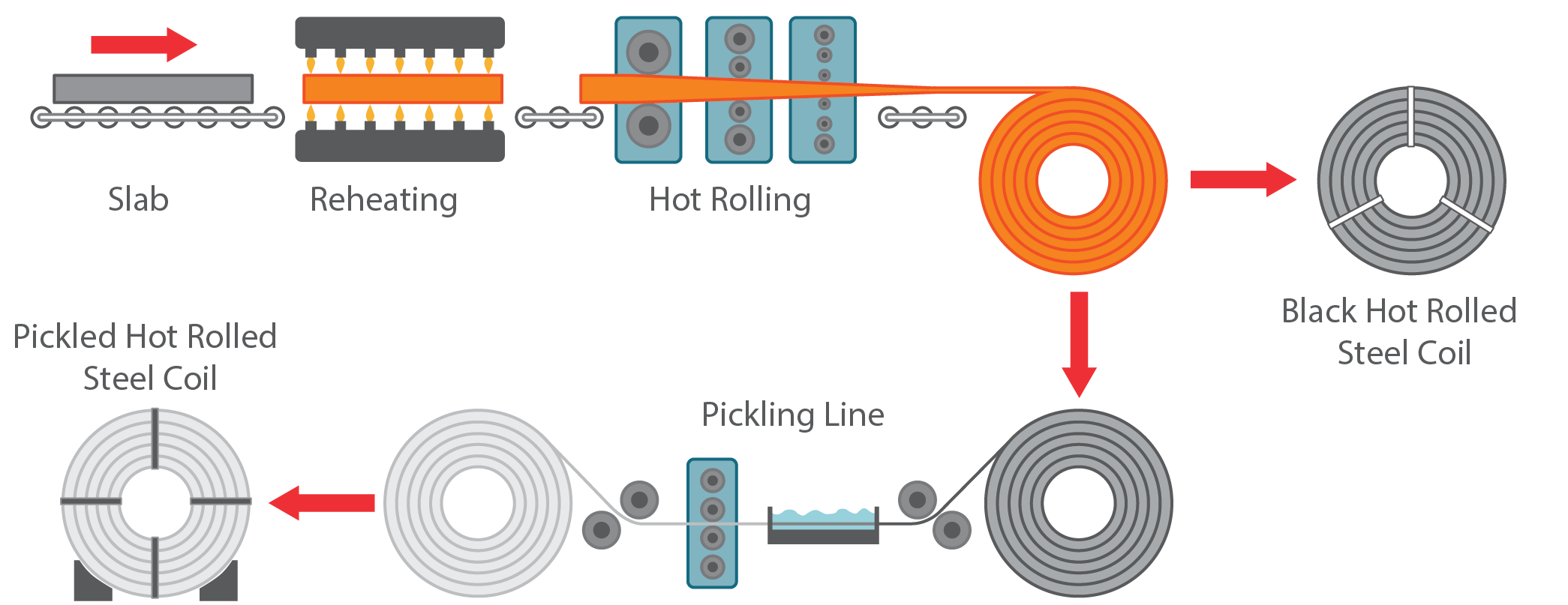
Failure Analysis of Corroded Steel Surface
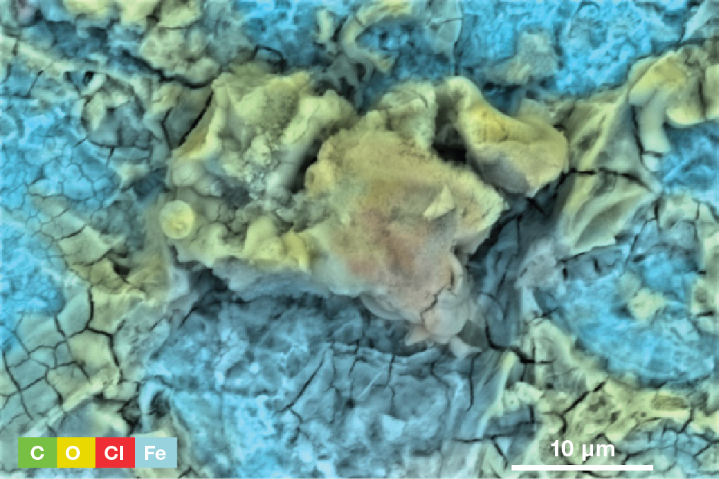
Hot-rolled steel sheets undergo a pickling process — acid bath dissolution — to remove the oxide scale formed during reheating. After the etching and washing steps, stain spots can appear on the pickled steel surface, requiring root cause investigation to prevent recurrence in production.
Using the Axia ChemiSEM, a contaminated etched steel surface was characterized to identify the cause of staining. In approximately one minute of analysis, a quantitative elemental map revealed that the stain region contained significant chlorine — unexpected on a washed steel surface. Region analysis confirmed the foreign particle contained 57.9 at.% oxygen and 9.8 at.% chlorine, compared to only 9.5 at.% oxygen and no detectable chlorine on clean etched steel. The conclusion: pickling acid droplets contacted the surface after the washing step, leaving chloride-rich residues. This finding was achieved within a single ChemiSEM session — no software switching, no image re-collection, no separate EDS acquisition required.
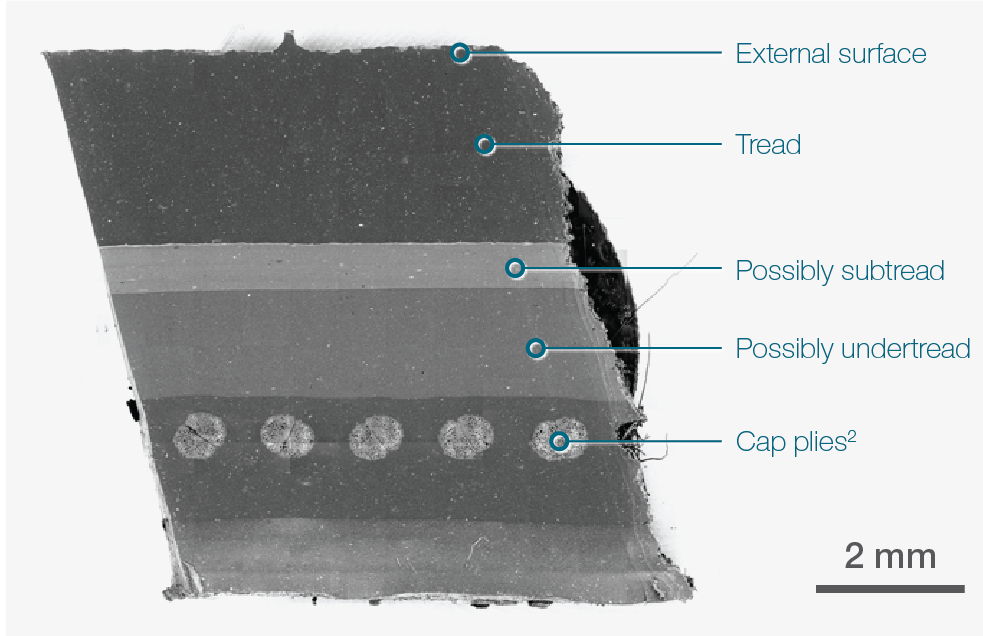
Characterization of Tire Fillers
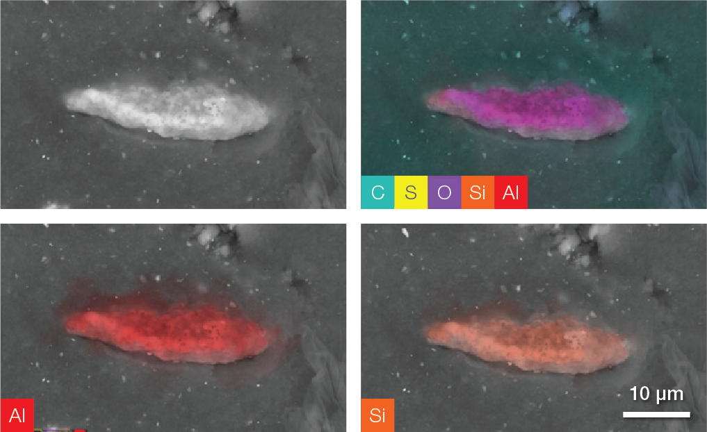
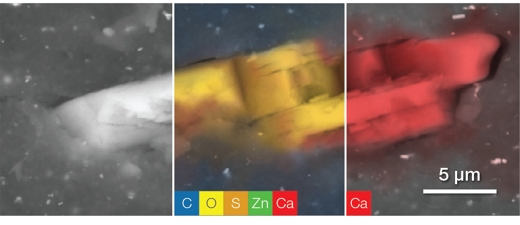
Tires are highly engineered structural composites containing up to 20 rubber compounds with varied microstructures. Reinforcing fillers — which can exceed 40% of the total tire compound — are critical to elastic efficiency and long-term performance. An optimal, homogeneous dispersion of all fillers is a key quality indicator; poor dispersion is directly linked to tire failure modes including tread detachment and premature aging.
Conventional BSE imaging is insufficient to differentiate the large variety of filler materials in modern tires, as many have similar atomic numbers. The Axia ChemiSEM resolves this limitation through live quantitative elemental mapping. A 19×19 tile navigation montage of a tire cross section was acquired in approximately 15 minutes at low vacuum (30 Pa), providing a complete large-area overview with simultaneous chemical context. Analysis identified zinc oxide (ZnO) clusters, aluminosilicate fillers (Al SiO ), calcium carbonate, and talc — each mapped by composition in a single acquisition pass without changing imaging methodology or conditions.
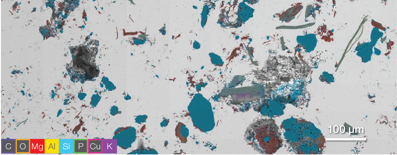
Malachite Characterization
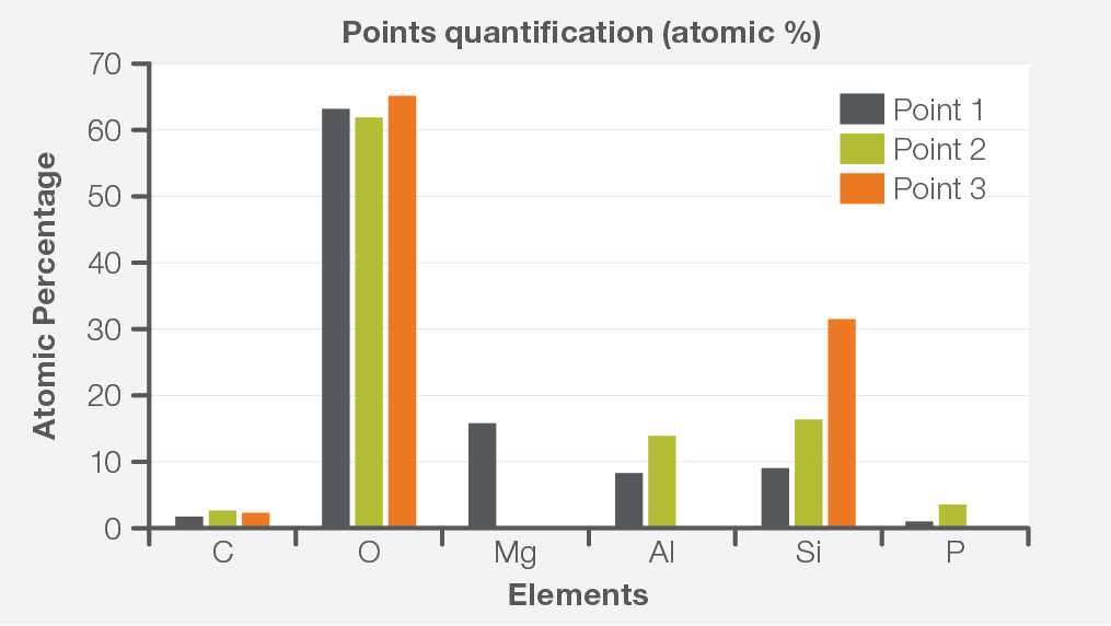
Malachite [Cu (CO )(OH) ] is a copper carbonate hydroxide mineral formed as a secondary mineral when copper minerals are altered by environmental chemicals. During formation, other elements such as Mg, Al, Si, and Fe can be incorporated as inclusions. Tracking the spatial relationships between chemistry and microstructure is key to interpreting the history of secondary mineralization and the relative timing of crystal growth.
The Axia ChemiSEM provides a new approach to mineral characterization. A large-scale chemical overview was acquired using Navigation Montage combined with live quantitative elemental mapping, providing a rapid picture of elemental distribution across the full sample surface. Within the same acquisition, individual elements could be selected or deselected to highlight compositional differences between regions indistinguishable by BSE contrast alone. Point & ID analyses confirmed at least three distinct phases — differentiated by Al, Mg, and Si distributions — within inclusions that appeared identical in conventional BSE imaging. The entire characterization from overview to point quantification was conducted in a single software environment without re-acquiring images or changing acquisition parameters.
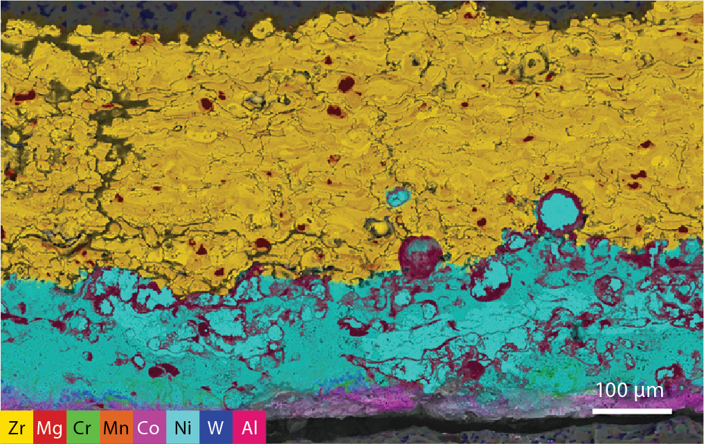
Thermally Cycled Thermal Barrier Coating System
Thermal barrier coatings (TBCs) are critical protective systems applied to aerospace engine components to enable operation at temperatures exceeding the limits of the underlying metal. A TBC system consists of a ceramic top coat (~500 μm), an oxidation-resistant metallic bond coat (~200 μm), and a Ni-based superalloy substrate — all of which must maintain integrity under extreme cyclic thermal loading up to 1700°C, such as in the Pratt & Whitney JT11D afterburner engine used in the SR-71 aircraft.
Characterization of a thermally fatigued TBC fragment — from an aircraft with more than 15,000 flight hours — was performed using the Axia ChemiSEM. A large-area ChemiSEM image was acquired by collecting a 7×7 tile montage with 5 integrated frames per ROI, completed in approximately 30 minutes. The resulting image simultaneously revealed the distribution of Zr, Mg, Cr, Mn, Co, Ni, W, and Al across all layers, immediately highlighting an inhomogeneous interface between the bond coat and top coat from extensive thermal cycling. This interface degradation — a precursor to delamination — was directly visible in the ChemiSEM image and guided subsequent high-magnification drift-corrected EDS analyses of the γ and γ' phases in the Ni-based superalloy.

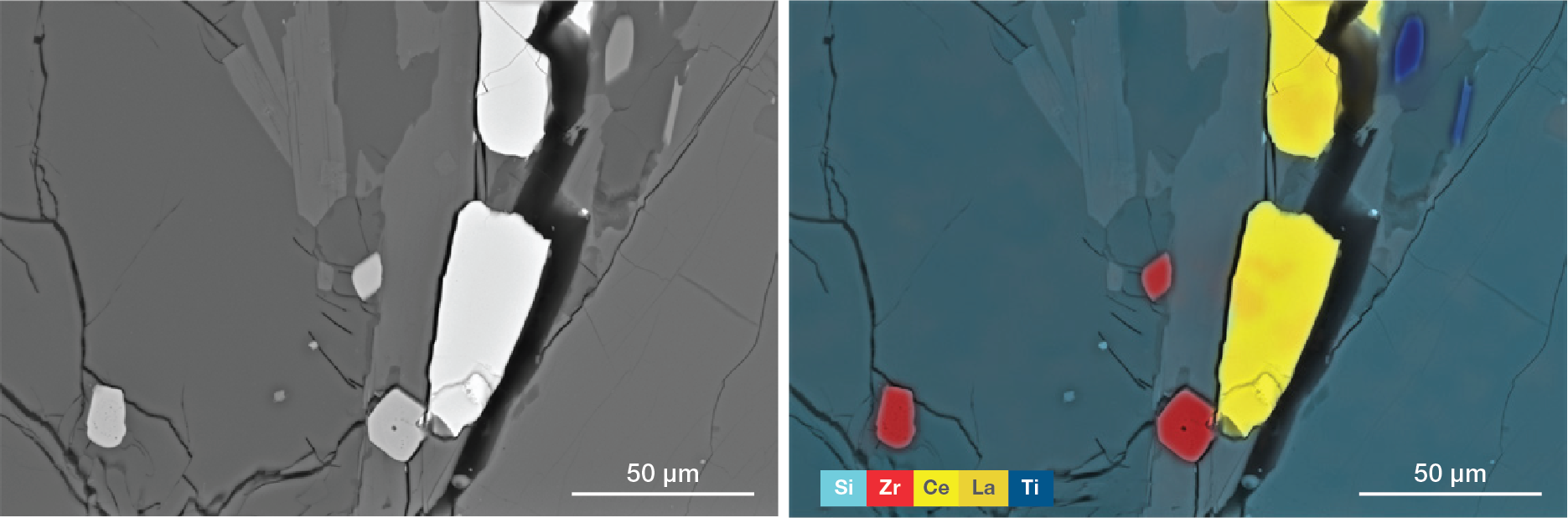
ChemiSEM for Geochronological Studies
U-Pb dating is the most widely applied age-determination method in metamorphic and igneous rock research. The target minerals — zircon, monazite, and titanite (5–60 μm) — preserve complex age domains recording geologically important events. A critical bottleneck in geochronological workflows is efficiently locating dateable mineral populations across large polished sample surfaces, as insufficient sampling leads to bias in age interpretation and provenance studies.
A new zircon and monazite dating protocol was developed using the Axia ChemiSEM, combining large-area ChemiSEM phase mapping with cathodoluminescence (CL) imaging. The three-step workflow begins with automated low-magnification SEM-EDS phase mapping of the entire sample, simultaneously highlighting the position of zircon (Zr), monazite (Ce, La), and titanite (Ti) across the full surface. This ChemiSEM overview navigates to the second step: high-magnification BSE imaging and ChemiSEM point & ID quantification of individual grains. The third step integrates CL imaging using the retractable solid-state CL detector (10 keV, four R-G-B-Pan channels) for textural information on zircon growth zones and crystal defects invisible to EDS. Combining ChemiSEM and CL in one workflow eliminates the need for separate instruments and dramatically increases the number of datable grains identified per session.