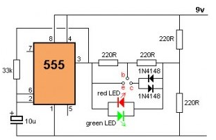
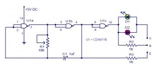
PNP Transistor Symbol and Structure; Transistor Tester Circuit Diagram
PNP Transistor Symbol and Structure; Transistor Tester Circuit Diagram
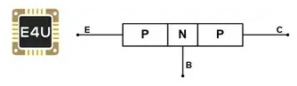
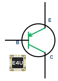
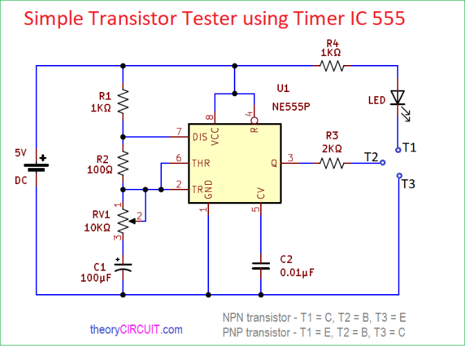
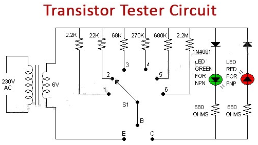
First, Overview of PNP Transistors A PNP transistor is a bipolar transistor used in electronic circuits for amplification, switching, and current control. Compared to an NPN transistor, a PNP transistor is characterized by its three distinct semiconductor regions: positive (P-type), negative (N-type), and positive (P-type). This structure causes the PNP transistor to differ from the NPN transistor in the direction of current flow and the type of charge, but their operating principle is essentially the same. The "PNP" in PNP transistor represents the three distinct semiconductor regions in its structure: positive (P-type), negative (N-type), and positive (P-type). The positive region is rich in positive charge and is usually made of materials such as silicon (Si), and is called the "base region" or "bottom region." The negative region is rich in negative charge and is also made of materials such as silicon, and is called the "emitter region." The second positive region is again rich in positive charge and is called the "collector region." When a positive voltage is applied to the base region, it attracts electrons from the emitter region to the base region, causing the PNP transistor to enter the conducting state. Electrons recombine in the base region and flow into the collector region, thus forming a current path. When a voltage is applied to the collector region, current flows out of the transistor. The magnitude of the current can be controlled by controlling the base voltage. Second, PNP Transistor Symbol and Structure The structure of a PNP transistor is similar to that of an NPN transistor. In an NPN transistor, a P-type semiconductor is sandwiched between two N-type semiconductors. In a PNP transistor, an N-type semiconductor is sandwiched between two P-type semiconductors. The structure of a PNP transistor is shown in the figure below. Basic Diagram of a PNP Transistor Construction of a PNP Transistor In P-type semiconductors, most charge carriers are holes. Therefore, in a PNP transistor, current is generated due to the movement of holes. The middle N-type layer is the base (B). The left P-type layer is the emitter (E), and the right P-type layer is the collector (C). Compared to the base (N-type) layer, the emitter and collector (P-type) layers are more heavily doped. Therefore, the depletion regions at both junctions penetrate more into the base layer. The areas of the emitter and collector layers are larger than those of the base layer. In N-type semiconductors, there are a large number of free electrons. However, the middle layer is very narrow and lightly doped. Therefore, there are significantly fewer free electrons in the base region. The symbol for a PNP transistor is shown in the diagram below. The arrows indicate that current flows from the emitter to the collector. PNP Transistor Symbol Third, PNP Transistor Testing Methods There are several methods for testing PNP transistors. Two commonly used methods will be detailed below. 1. Testing with a Digital Multimeter (1) Identifying the Base First, set the digital multimeter to diode mode. Connect the red probe to any pin, and then connect the black probe to the other two pins in sequence. If both readings are less than 1V or both display an overflow symbol "1", then the pin connected to the red probe is the base (B). (2) Determining the Transistor Type After identifying the base (B), connect the red probe to the base (B), and then connect the black probe to the other two pins in sequence. If both readings are 0.500–0.800V, the transistor is NPN; if both readings are an overflow symbol "1", then the transistor is PNP. (3) Testing Pin Functions For PNP transistors, hold the positive (red) probe of the multimeter on the LEFT pin of the transistor and the negative (black) probe on the MIDDLE pin, and read the value. Then, hold the positive (red) probe on the RIGHT pin of the transistor and read the value again. When comparing the two readings, the pn junction with the higher reading is the base-emitter junction, while the pn junction with the lower value is the collector-base junction. 2. Testing with a Transistor Curve Tracer (1) Instrument Setup When using a transistor curve tracer, first set the instrument to its initial position according to the model and parameters of the transistor being tested. For example, when testing a PNP transistor, the switch should be in the negative position. Simultaneously, adjust all the collector scan knobs to the required range, as well as the sensitivity of the X and Y axes. (2) Testing Process Connect the transistor's pins to the corresponding interface on the curve tracer and begin the test. During the test, the transistor's characteristic curve can be observed, and the transistor's operating state can be determined based on the curve. (3) Precautions During the test, pay attention to the transistor's temperature, power consumption, and other parameters to avoid exceeding their limits and damaging the transistor. After the test, reset the instrument and store it properly. PNP transistors, as important electronic devices, play a crucial role in electronic circuits, performing amplification, switching, and current control. Understanding their structural characteristics and working principles, as well as mastering correct testing methods, allows us to better use and maintain PNP transistors, ensuring the stability and reliability of electronic circuits. Furthermore, with the continuous advancement and development of technology, we believe that more new electronic devices and technologies will emerge, injecting new vitality into the electronics industry. Fourth, Transistor Tester Circuit Diagram 1. Transistor Tester Circuit Diagram Using a 555 Timer IC This transistor test circuit uses a 555 timer IC and is suitable for testing PNP and NPN transistors. Compared to other transistor testers, this circuit is very simple, making it useful for technicians and students. It can be easily built on a general-purpose PCB. Basic electronic components such as resistors, diodes, LEDs, and the NE5555 timer are used in developing this circuit. Using this circuit, various faults can be checked—for example, whether the transistor is in good condition, open-circuited, or short-circuited. The NE555 timer IC is a multivibrator with three operating modes: astable, monostable, and bistable. In addition, the circuit can operate for extended periods using a battery. The transistor test circuit operates at a frequency of 2Hz. Output pin 3 applies a positive voltage to the transistor test circuit, followed by a non-zero voltage. At the other end of the circuit, a voltage divider is connected at approximately 4.5V midpoint, resulting in the following: When no transistor is connected to the tester, the green and red LEDs blink alternately. When the transistor is placed on the test lead, both LEDs blink. If only one LED blinks, the transistor is functioning correctly. If the voltage is only in one direction, a short circuit will occur between the LED pairs. If neither LED blinks, the transistor will be short-circuited; if both LEDs blink, the transistor will be open-circuited. 2. LED-based Transistor Tester Circuit Diagram The above is a simple transistor tester circuit; the Quad2 input CMOS, NAND gate IC, and CD4011B are the core components. In this circuit, we use two LEDs to indicate the status. Using this circuit, we can test PNP and NPN transistors. Internally, only three of the four NAND gates are used. These gates are used as NOT gates by shorting their input terminals. Here, resistor R1, capacitor C1, and gates U1a and U1b form a square wave oscillator. The frequency of this oscillator is adjusted by resistor R1, and the oscillator output is inverted by gate U1c. The inverting and non-inverting oscillator outputs are connected to the base of the transistor under test through resistors R2 and R3. During the test, the LED status indicates the transistor's condition. If the red LED is lit, the NPN transistor is good. If the green LED is lit, the PNP transistor is good. If both LEDs are lit, the transistor under test is short-circuited. If both LEDs are off, the transistor under test is open-circuited or damaged. Therefore, this is all there is to transistor tester circuits and digital multimeters. Transistor testers have the necessary switches and controls for proper current, voltage, and signal settings. Furthermore, these transistor testers are designed to check solid-state diodes. There are also preferred testers for checking high-voltage transistors and rectifiers. Most circuits are designed with transistors, and many circuits and prototypes use transistors with different parameters. If you are debugging a circuit to find a fault, in most cases you must check the condition of the transistors; similarly, it is best to test and implement transistors in the circuit. 3. Transistor Tester Circuit Using a 555 Timer Here is a simple transistor test circuit designed using a 555 timer to test all types of transistors. The schematic has an LED indicator that flashes if the transistor is working well and remains off if the transistor is open or not working. This circuit uses a 555 timer transistor test circuit as an astable multivibrator circuit, generating a square wave pulse output based on the timing resistor and timing capacitor values. The circuit output is connected to test point T2, the positive power supply is connected to test point T1 through resistor R4 and the LED, and the negative power supply is connected to test point T3. We know that each transistor acts as a switch. Here, an NPN or PNP transistor is placed at the test point. The output pulse from the astable multivibrator drives the base of the test transistor, causing it to repeatedly turn on and off. Therefore, the LED starts blinking. If this happens, it can be considered a working transistor. If the test transistor is on or not working, the LED remains off. Before testing an unknown transistor, use a known good transistor (NPN and PNP) test circuit. Place the correct pins at the test points and check the transistor datasheet for the accurate pin configuration. 4. Simple Transistor Tester Circuit Diagram Transistors are the most commonly used components in electronic products, but they are prone to failure. You must check the operation of transistors with a multimeter. This can be very time-consuming, involving testing each terminal one by one. Understanding and designing these multimeters and transistor testers can be complex. However, in this tutorial, we'll build a simple transistor test circuit that can test both PNP and NPN transistors. This circuit is simple to build and very convenient for testing transistors. It uses two different LEDs to indicate the transistor's operating status: one for NPN transistors and the other for PNP transistors. As is known, a transistor has three terminals: base, emitter, and collector. To connect the transistor to this circuit, we have marked three points in the circuit diagram, as you can see. It is crucial to place the transistor leads in the correct orientation. The transistor emitter is connected to the circuit emitter, where (E) is marked. The transistor base is connected to the circuit base (where marked (B)) and the transistor collector is connected to the circuit collector, marked C. If these are not connected to their respective points, the circuit will not give accurate results. The 230V AC power from the mains supply is stepped down to the required operating voltage (6 volts) by a transformer. Different resistors are used in this circuit as current limiters for the transistor being tested. A rotary switch S1 is used to select the correct base resistor for the transistor. We use two LEDs in this circuit. The NPN transistor uses a green LED, and the PNP transistor uses a red LED. Each LED is connected to a resistor to limit the base current. When the NPN transistor is operating normally, the green LED lights up; when the PNP transistor is operating normally, the red LED lights up.