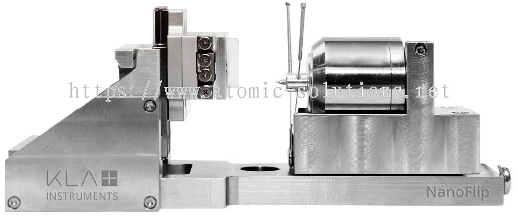

NanoFlip
Universal nanomechanical tester with a flip mechanism that transitions between imaging and testing. Measures hardness, modulus, yield strength, stiffness and other nanomechanical properties with high accuracy and precision under both ambient and vacuum conditions.
Product Overview
The NanoFlip provides rapid results by synchronizing SEM images with mechanical test data. Modular options accommodate a variety of applications such as mechanical property maps, frequency-specific dynamic tests, and scratch and wear. The system is powered by electromagnetic transducers to deliver precise measurements and avoid artifacts in the x and y axes. In its standard configuration, the NanoFlip utilizes the InForce 50 force actuator with a modular controller design optimized for upgrades. The system conforms to ISO 14577 to ensure data integrity. The proprietary InView software suite includes RunTest for simplified test setup, ReviewData for data analysis, and InFocus for generating presentation-quality graphs and reports.
Main Features & Capabilities
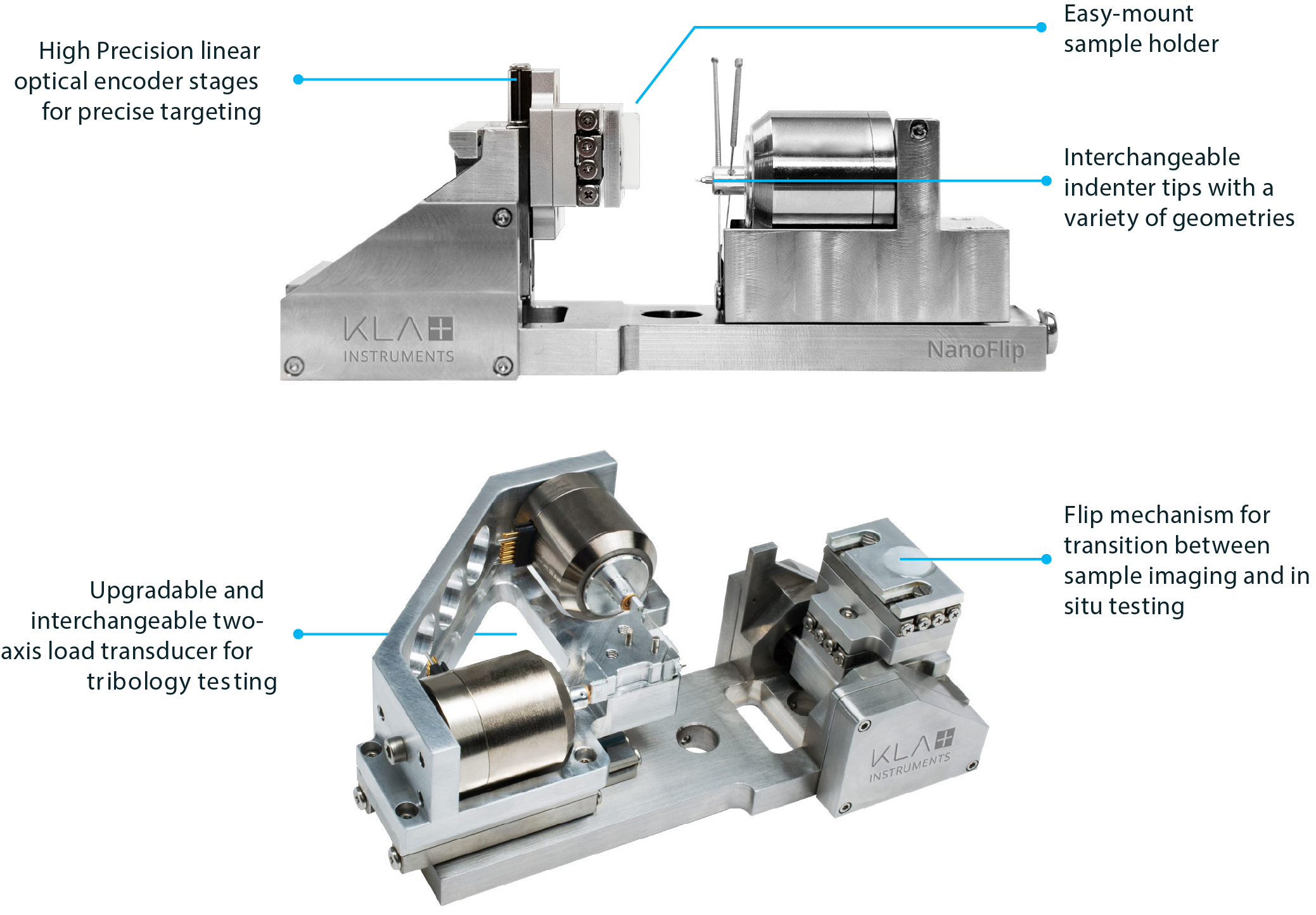
Flip Mechanism for In Situ Testing
Revolutionary FIB-to-test technology enables seamless transition from FIB to indentation by tilting the sample 90°, allowing combined imaging and mechanical testing without sample transfer.
High-Speed Data Acquisition
Controller electronics with 100kHz data acquisition rate and 20µs time constant capture nanoscale changes in mechanical properties during contact for high-resolution dynamic testing.
SEM Video Synchronization
Integrated SEM video capture provides synchronized SEM images with test data, linking SEM-recorded video to nanoscale changes in mechanical properties for comprehensive analysis.
Pre-Programmed Test Methods
Large suite of pre-programmed nanomechanical test methods for improved ease-of-use, plus proprietary online nanoindentation courses taught by nanoindenter experts.
Modular Upgradeable Platform
Upgradeable, extendible platform for automated nanoindentation testing with interchangeable two-axis load transducer for tribology and lateral force measurement.
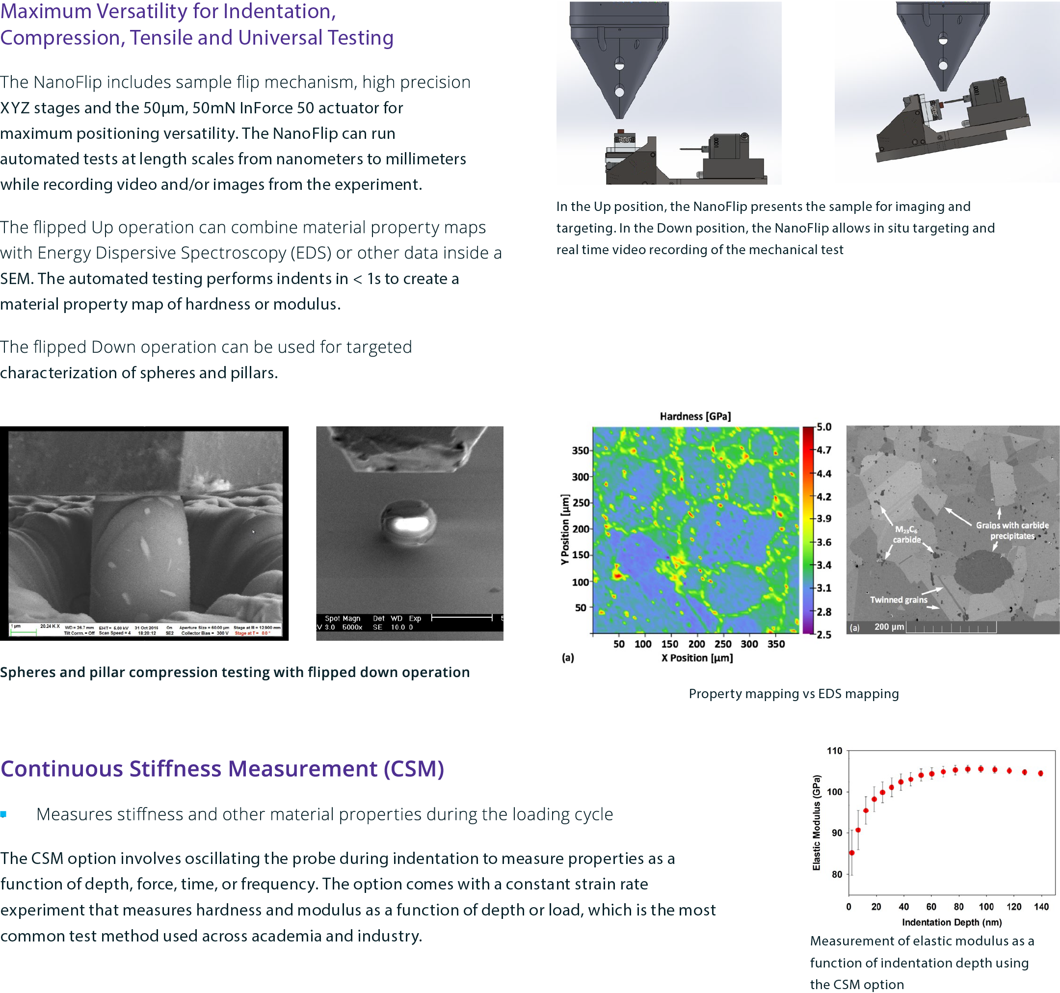
Continuous Stiffness Measurement
The CSM option oscillates the probe during indentation to measure stiffness and material properties as a function of depth, force, time, or frequency throughout the loading cycle.
Description & Key Benefits

Versatile Applications
MEMS & Nanoscale Devices
Micropillars, nanoscale devices and micro-electromechanical systems requiring high-precision nanoindentation for hardness, modulus and stiffness characterization.
Metals & Alloys
Bulk and thin-film metallic specimens requiring nanomechanical property measurement under both ambient and vacuum conditions for material science research.
Batteries & Energy Storage
Glove-box compatible for inert environment applications such as battery electrode and electrolyte testing with nanomechanical characterization.
Semiconductor Packaging
Packaging materials, interconnects and thin films in semiconductor devices requiring precise modulus and hardness mapping with NanoBlitz rapid property mapping.
Polymer & Plastics
Soft polymers and other materials with sample geometries or volumes not suitable for standard DMA tests, characterized using ProbeDMA dynamic mechanical analysis.
