详情
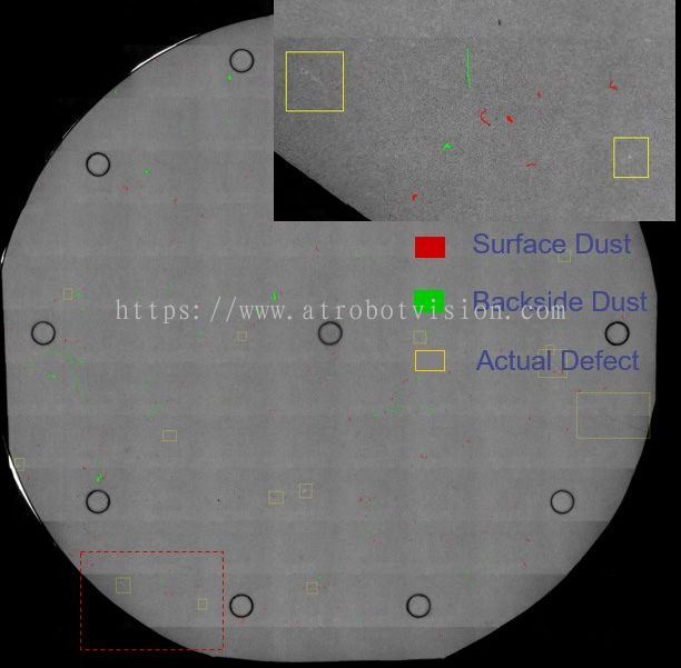
The optical inspection of patterned wafers can employ bright-field illumination, dark-field illumination, or a combination of both for defect detection. Patterned wafer inspection systems compare the image of a test die on the wafer with that of an adjacent die (or of a "golden" die known to be defect free).
更多 Atrobot Sdn. Bhd. 相关资料
 Malaysia