详情
BUY NJM4565DD https://www.utsource.net/itm/p/53749.html
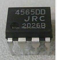
DUAL OPERATIONAL AMPLIFIER??
| Parameter |
Symbol |
Conditions |
Min |
Typ |
Max |
Unit |
| Supply Voltage |
VCC |
- |
1.8 |
- |
5.5 |
V |
| Quiescent Current |
ICC |
VCC = 5V, no load |
- |
100 |
- |
μA |
| Output Voltage Swing |
VOUT |
VCC = 5V, RL = 1kΩ |
0.2 |
- |
4.8 |
V |
| Input Offset Voltage |
VIO |
- |
- |
5 |
- |
mV |
| Input Bias Current |
IIB |
- |
- |
100 |
- |
nA |
| Slew Rate |
SR |
- |
- |
0.3 |
- |
V/μs |
| Bandwidth (Unity Gain) |
fBW |
- |
- |
1 |
- |
MHz |
| Open Loop Gain |
AVOL |
- |
- |
100 |
- |
dB |
| Common Mode Input Range |
VCM |
- |
0 |
- |
VCC - 1.2 |
V |
| Output Short-Circuit Protection |
- |
- |
Yes |
- |
- |
- |
| Operating Temperature |
TOP |
- |
-40 |
- |
85 |
°C |
Instructions for Using NJM4565DD
Power Supply:
- The NJM4565DD operates with a supply voltage ranging from 1.8V to 5.5V. Ensure that the power supply is stable and within this range to avoid damage or erratic behavior.
Quiescent Current:
- The quiescent current is typically 100 μA at 5V. This value should be considered when designing circuits to ensure efficient power usage.
Output Voltage Swing:
- The output voltage swing is from 0.2V to 4.8V when the supply voltage is 5V and the load resistance is 1kΩ. Ensure that your load does not exceed these limits to avoid distortion.
Input Offset Voltage:
- The typical input offset voltage is 5 mV. This can affect the accuracy of the amplifier, so it may need to be compensated for in precision applications.
Input Bias Current:
- The typical input bias current is 100 nA. This should be taken into account when designing input circuits to prevent unwanted loading effects.
Slew Rate:
- The typical slew rate is 0.3 V/μs. This limits the maximum rate of change of the output voltage and can affect the performance in high-frequency applications.
Bandwidth:
- The unity gain bandwidth is typically 1 MHz. This determines the frequency range over which the amplifier can operate effectively.
Open Loop Gain:
- The open loop gain is typically 100 dB. This high gain allows for precise control of the output when used in feedback configurations.
Common Mode Input Range:
- The common mode input range extends from 0V to VCC - 1.2V. Inputs outside this range can lead to incorrect operation.
Output Short-Circuit Protection:
- The NJM4565DD has built-in output short-circuit protection. However, prolonged short circuits can still cause damage, so it is advisable to include external protection measures.
Operating Temperature:
- The operating temperature range is from -40°C to 85°C. Ensure that the device is used within this range to maintain reliable performance.
Handling and Storage:
- Handle the NJM4565DD with care to avoid static damage. Store in a dry, cool place to prevent moisture-related issues.
Circuit Design:
- Use appropriate decoupling capacitors (e.g., 0.1 μF and 10 μF) near the power supply pins to reduce noise and improve stability.
- Ensure that all connections are secure and free from solder bridges or other defects.
By following these guidelines, you can ensure optimal performance and reliability of the NJM4565DD in your electronic designs.
(For reference only)
更多 Utsource Holding Company Limited 相关资料